Hubei Hannas Tech Co.,Ltd-Professional Piezoceramic Elements Supplier
Hot Keywords:
- All
- Product Name
- Product Keyword
- Product Model
- Product Summary
- Product Description
- Multi Field Search

Views: 2 Author: Site Editor Publish Time: 2020-03-16 Origin: Site


Piezoelectric ceramic micro-actuators are new type solid-state actuators made using the inverse piezoelectric effect. They are widely used in high tech fields such as precision optics, micromechanics, microelectronics, and computer applications. These applications require piezoelectric ceramic devices to be small , Low driving voltage, large displacement, and integration. In the past, multilayer piezoelectric ceramic microactuators formed by bonding piezoelectric ceramic with an adhesive have been affected by the thickness of the single ceramic diaphragm. Limitation (It is quite difficult to make a ceramic monolithic with a thickness of 200 μm or less), the device cannot be miniaturized and integrated, and the adhesive in the device becauses the device generate large creep under the action of an electric field, which is not conducive to the precision of displacement control, especially the device under the action of high electric field for a long time, the adhesive is easy to fall off from the piezo ring welding componnets sheet, causing the device performance to deteriorate, and even the device fracture phenomenon, shortening the device's service life, bringing great benefits to the application. In recent years, the multilayer chip piezoelectric ceramics obtained by using the green casting process of piezoceramics and the co-firing technology of the cast piezoceramics green film and the internal electrode ceramic micro-actuator (MMPA) is a new type of functional ceramic device with excellent performance suitable for large-scale production. This multilayer chip device is easy to produce a film thickness of less than 100 μm due to the casting process. After firing, the piezo ceramic layers are directly bonded to the internal electrode without the need for adhesive bonding. Therefore, the device can be miniaturized and miniaturized, the creep performance of the device is also greatly improved, and the layering phenomenon between the ceramic layers is greatly improved. It is effectively overcome, which greatly improves the service life of the device. This article reports a multilayer chip type and high lead PZT system pressure made by using ceramic casting technology and ceramic green film / metal internal electrode co-firing technology. This is the first time for an electric ceramic micro-actuator in this country. This paper mainly studies the static and dynamic displacement characteristics of this device.
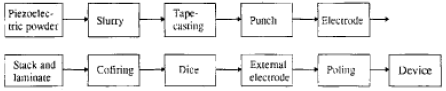
The process flow for preparing a multilayer chip piezoelectric ceramic micro-actuator needs to go through 10 main process steps: first, a soft PZT ternary piezoelectric ceramic powder with a large piezoelectric strain coefficient is prepared by an electronic piezo ceramics preparation process, The molecular formula is xPb(Zn1/3Nb2/3)O3+yPbZrO3+zPbTiO3,(PZN-PZ-PT), (x+y+z=1),
Then, the pzt ceramic powder and the organic additive are mixed uniformly in a certain solid / liquid ratio to obtain a uniform ceramic slurry, and the ceramic slurry is cast in a hopper on a casting machine for casting. And organic carrier speed to prepare a uniform, dense, cast green film with a certain thickness. The cast green film is punched into a pzt ceramic green film of a certain shape, and a pattern with a pattern electrode paste, and then the ceramic green film printed with electrodes is placed in a special mold and laminated in a certain order to obtain a multilayer piezo ceramic. After cutting the multilayer body of multiple multilayer ceramic devices according to the size of the device's active area, put them into a pure Al2O3 crucible and slowly pack them together.The two ends of the multilayer chip device are covered with Ag external electrodes, 650 C silver burned, high temperature polarization (polarization time 30min, electric field 4000V / mm, temperature 140 C). Convection thick film and high temperature internal electrode, and finally obtained a multilayer chip piezoelectric ceramic micro-actuator with an active area of 5mm × 6mm and a total thickness of 2mm (the piezoelectric ceramic layer is 35 layers, each layer is 47 μm thick and the upper and lower surface layers are about 120 μm thick) .
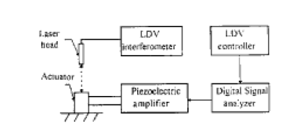
The piezoelectric strain d33 coefficient of the piezo ceramic componnets was measured by the Institute of Acoustics of the Chinese Academy of Sciences. The micro-area microstructure of the multilayer device was observed with a scanning electron microscope (SEM) produced by the Instrument Factory of the Chinese Academy of Sciences. The displacement value of the electric ceramic micro-actuator is tested by the DGS-6 digital display inductance tester produced. The resolution is 0.01 μm. The dynamic displacement is tested by a single laser beam according to the principle of the doppel effect. The resolution is 0.005μm.
For a piezoelectric ceramics are subject to constant external stress, when a voltage is applied to two surfaces perpendicular to its thickness direction (polarization direction), and considering only piezoelectric deformation to linear deformation, it can be known from the piezoelectric equation that the pressure.The displacement Δll of the electric ceramic in the longitudinal thickness direction is expressed.
Where d33 is the piezoelectric strain coefficient, V is the applied voltage, and t is the thickness of the ceramic monolith. Equation shows that when the applied voltage is the amount of change, the displacement of the piezoelectric sheet in the thickness direction and the piezoelectric .The strain coefficient d33 is proportional to the applied voltage V and has nothing to do with the thickness; however, when the applied electric field is changed, the displacement generated by the device is not only proportional to the piezoelectric coefficient d33 and the electric field, but also proportional to the thickness It is proportional. It can be seen that the displacement of the piezoelectric ceramic in the thickness direction is related to the working mode of the displacement drive selected by the piezoelectric ceramic. When is applying, the two factors of the applied voltage and electric field should be considered at the same time. Application under near-breakdown electric field; at the same time, the working voltage should be as low as possible, and the displacement should be as large as possible.
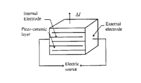
For a device with a certain applied voltage, reducing the thickness of the ceramic sheet can achieve the purpose of reducing the size of the device in the thickness direction. Therefore, when the multilayer piezoceramic sheet is mechanically connected in series, electrically connected in parallel, and the piezo ceramic layer together, the polarization direction of adjacent piezo ceramic transducer takes the reverse structure. In this way, when the multilayer piezoelectric ceramic micro-driver is applied with an operating voltage, its longitudinal displacement is superimposed, which can be expressed .
Where N is the number of piezo ceramic laminates, that is, the displacement of the multilayer piezoelectric ceramic micro-actuator is enlarged by N times compared with a single piece of piezoelectric ceramic. However, when the displacement is based on the electric field applied by each piezoelectric ceramic sheet When the amount of change is, equation (2) can be expressed .
Where t is the thickness of each layer of piezoelectric ceramics, and l is the total thickness of the multilayer device. Comparing the expressions of equations (3) and (1), it can be found that when is the total thickness of the multilayer device. When the thickness t is the same, the two equations are the same, which indicates that when the electric field intensity applied by each piezoelectric ceramic piece of the multilayer device is the same as that of a single piece of piezoelectric ceramic, the displacement amount of the two is equal. The applied voltage is N times lower than that of a monolithic piezoelectric ceramic.
It can be seen from the above analysis that although monolithic piezoelectric ceramics can also achieve micron-scale displacement by increasing the film thickness, the applied working voltage needs to be thousands of volts, which is not conducive to application. As the amount of change, it has two different functions of amplifying the amount of displacement and reducing the operating voltage. Especially when the multilayer device keeps the electric field constant, the total thickness can be increased by increasing the number of layers of the device. Therefore, it is practically applied. When multi-layer devices not only havve an enlarged displacement, but also can effectively reduce the operating voltage.
the total thickness is 2 mm (the piezoelectric ceramic layer is 35 layers, each layer is 47 μm thick, and the upper and lower surface layers are each about 120 μm thick), which is prepared by the ceramic blank film casting process and the ceramic / metal internal electrode co-firing technology. The white parallel stripes in the picture are metal internal electrodes with pzt ceramic layers between the internal electrodes. Many pores with a size of several microns can be observed in the piezo ceramic ring. This is due to the ceramic casting. Organic materials such as binders and plasticizers occupy a certain proportion in the green film. When the ceramics / internal electrodes are co-fired, the volatilization of the organic materials in these films causes many large pores in the pzt ceramic layer. However, these pores are in the PZT series. The electromechanical characteristics of the pzt ceramic layer are not seriously affected in the cast ceramic sheet. This result is basically consistent with the electromechanical coefficient of the PBNN rigid piezoelectric ceramics prepared by the casting method. Therefore, it can be considered that the electromechanical parameters of the piezo ceramic obtained by the casting method are basically the same as those of the ceramic sheet by the dry pressing method.
 Tech Co,.Ltd")


